Product Summary
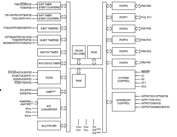
The UPD78F9177AYGB-8ES-A is μPD789177, 789177Y Subseries (small, general-purpose) in the 78K/0S Series. The UPD78F9177AYGB-8ES-A replaces the internal ROM of the μPD789176 and μPD789177 with flash memory. Because flash memory allows the program to be written and erased electrically with the μPD78F9177 mounted on the board, this product is ideal for the evolution stages of system development, small-scale production and rapid development of new products.
Parametrics
UPD78F9177AYGB-8ES-A absolute maximum ratings: (1)Supply voltage, VPP: -0.3 to +10.5 V; (2)VI1 Pins other than P50 to P53, P23, P24: -0.3 to VDD + 0.3V; VI2 P23, P24: -0.3 to +5.5 V; (3)Input voltage, VI3 P50 to P53: -0.3 to +13 V; (4)Output voltage VO: -0.3 to VDD + 0.3 V; (5)Output current, high IOH Per pin: -10 mA; (6)Total for all pins: -30 mA; (7)Output current, low IOL Per pin: 30 mA; Total for all pins: 160 mA; (8)Operating ambient temperature TA In normal operation mode: -40 to +85 ℃; During flash memory programming: +10 to +40 ℃; (9)Storage temperature Tstg: -40 to +125 ℃.
Features
UPD78F9177AYGB-8ES-A features: (1)Pin compatible with mask ROM version (except VPP pin); (2)Flash memory: 24 Kbytes; (3)High-speed RAM: 512 bytes; (4)Minimum instruction execution time can be changed from high-speed (0.4 ms: @5.0-MHz operation with main system clock) to ultra-low-speed (122 ms: @ 32.768-kHz operation with subsystem clock); (5)10-bit resolution A/D converter: 8 channels; (6)I/O ports: 31; (7)Serial interface: 2 channels; (8)Timers: 6 channels; (9)On-chip 16-bit multiplier; (10)Power supply voltage: VDD = 1.8 to 5.5 V.
Diagrams

 |
 UPD70008AG-4 |
 Other |
 |
 Data Sheet |
 Negotiable |
|
||||
 |
 UPD70236AGD-10-5BB |
 Other |
 |
 Data Sheet |
 Negotiable |
|
||||
 |
 UPD7030025AGC-25 |
 Other |
 |
 Data Sheet |
 Negotiable |
|
||||
 |
 UPD703014A |
 Other |
 |
 Data Sheet |
 Negotiable |
|
||||
 |
 UPD703014AY |
 Other |
 |
 Data Sheet |
 Negotiable |
|
||||
 |
 UPD703015A |
 Other |
 |
 Data Sheet |
 Negotiable |
|
||||
 (China (Mainland))


